C3Nano Wins Against Cambrios Advanced Materials in U.S. Patent Court

Cambrios Attempt to Invalidate C3Nano’s NanoGlue™ Patent Fails Before U.S. Patent Trials and Appeals Board

HAYWARD, CA – August 15, 2019 – C3Nano Inc., the world’s performance leader in silver nanowire-based transparent conductive inks and films used in flexible displays, touchscreens and other products, today announced that it has defeated an attempt by Cambrios Advanced Materials (CAM) to invalidate US Patent No. 9,183,968, one of several key patents in C3Nano’s extensive international intellectual property (IP) portfolio related to its proprietary NanoGlue™ fusing technology, which is required to achieve optimal performance for nanoscale metallic transparent conductors. C3Nano thus maintains the world’s most important IP portfolio related to silver nanowire-based transparent conductive inks and films, and once again demonstrates its unique advantages and industry leadership.

On August 9, 2019, the U.S. Patent Trials and Appeals Board rejected institution of inter partes review (IPR) requested in a Petition filed by CAM on February 1, 2019.  The denial of institution issued by the Board brings an end to the proceeding filed by CAM. The Board ruled that the arguments presented by CAM failed to meet the standard of a reasonable likelihood that the Petitioner (CAM) would prevail to establish invalidity of commercially significant claims and intellectual property.

NanoGlue technology is the key differentiator enabling the use of silver nanowire-based conductive films and inks for advanced commercial applications such as ultra-high resolution flexible screens, curved screens, wearables, and other next-generation display products.

In early 2019, CAM also withdrew two invalidation proceedings filed in China attempting to invalidate two of C3Nano’s Chinese patents (‘555 and ‘557) after having difficulty presenting its case to the Chinese patent review authorities.  CAM’s inability to maintain and support the withdrawn or rejected challenges to C3Nano’s patents demonstrates the superiority of C3Nano’s NanoGlue technology, and CAM’s repeated attempts to challenge C3Nano patents demonstrates the commercial viability of C3Nano technology over CAM.

“C3Nano is the only AgNW-based ink or film that is in mass production in flexible displays and phones. Cambrios has resorted to misguided and wasteful efforts, such as trying and failing to invalidate our IP in both the USA and China in an attempt to confuse and threaten our customers,” said Cliff Morris, CEO of C3Nano. “Our transformative advances in technology and patent protection ensure our continuing market leadership.”

Through customer wins and partnerships—such as the recent news that Hitachi Chemical Company qualified C3Nano’s ActiveGrid™ ink for mass production and is integrated in several flexible display devices in 2019—C3Nano is extending its lead for the commercialization of silver nanowire-based inks and films. C3Nano will continue to vigorously defend its valuable global intellectual property rights, and the company is committed to providing the highest performing materials for new generations of display products through its production facilities in Hayward, Calif., and Changzhou, China.

Related Content

Press Release
C3Nano Announces Scaling-Up of its Ultra-Nanowires™ Product Line: Plating Technologies Propel Nanowires to a New Level and Enable Novel Industrial Applications
More Robust and Reliable Nanowire Opens Countless New Conductive Composite and Coating Applications for Smart Adhesives, Aerospace, Anti-Static, Shielding, Biocompatibility, Heating, Automotives and Cleantech...
Press Release
C3Nano Announces Activegrid™ Room Temperature Curing Conductive Ink, Transforming the Advances Materials and Smart Surface Industry
New Low Temperature Process with Electrically Conductive Inks Unlocks Unprecedented New Application Possibilities for Life-Sciences, Packaging, Consumer Electronics, Automotive and Disposable Commodities October 04,...
Press Release
ACS announces winner of the ACS Central Science Disruptors & Innovators Prize
WASHINGTON, July 2, 2020 — The American Chemical Society (ACS) Publications Division and ACS Central Science are pleased to announce the winner of theACS Central Science Disruptors...
Press Release
C3Nano专利 情况说明
作为下一代透明导电油墨和薄膜的性能领导者,C3Nano公司就近期在中国的专利相关纠纷进展情况发表正式声明。
Press Release
C3Nano IP Positioning Statement
C3Nano Inc., the performance leader in next-generation, transparent conductive inks and films, would like to set the record straight with regard to recent IP developments...
Press Release
C3Nano FAQ With Regard to Its IP
FAQ Analysis: June 2020 1. Explain the difference between invalidation versus infringement. 2. Is C3Nano’s fusing technology/IP still protected? 3. The Cambrios press release...

C3Nano Scales Up Display Material Manufacturing with New Facility

US Facility Increases ActiveGrid™ Ink Manufacturing Capacity by Up to 10X

HAYWARD, CA – June 11, 2019 – C3Nano Inc., the world’s performance leader in silver nanowire-based transparent conductive inks and films used in flexible displays, touchscreens and other products, today announced that it has significantly increased its manufacturing capacity with the opening of a new facility in Hayward, California. C3Nano experienced 250 percent year-over-year growth in Q1 of this year and forecasts even greater growth in the near future, and this new facility increases the company’s manufacturing capacity tenfold.

The new 6,500 square-foot facility will house synthesis reactors, purification equipment, ink blending reactors and quality control instruments and will enable C3Nano to ship 140,000 kg of its ActiveGrid™ ink per year – enough to coat 9.8 million square meters of display film. This capacity will be needed to satisfy skyrocketing demand for highly interactive flexible displays in smartphones, tablets, wearables, and other devices.

“The device market is moving rapidly toward flexible and highly interactive displays, and silver nanowire-based inks and film are the preferred materials for these displays,” said Cliff Morris, CEO of C3Nano. “As the performance leader in silver nanowire-based inks and films, we are scaling up manufacturing to meet high demand for our products in Asia and around the world.”

Related Content

Press Release
C3Nano Announces Scaling-Up of its Ultra-Nanowires™ Product Line: Plating Technologies Propel Nanowires to a New Level and Enable Novel Industrial Applications
More Robust and Reliable Nanowire Opens Countless New Conductive Composite and Coating Applications for Smart Adhesives, Aerospace, Anti-Static, Shielding, Biocompatibility, Heating, Automotives and Cleantech...
Press Release
C3Nano Announces Activegrid™ Room Temperature Curing Conductive Ink, Transforming the Advances Materials and Smart Surface Industry
New Low Temperature Process with Electrically Conductive Inks Unlocks Unprecedented New Application Possibilities for Life-Sciences, Packaging, Consumer Electronics, Automotive and Disposable Commodities October 04,...
Press Release
ACS announces winner of the ACS Central Science Disruptors & Innovators Prize
WASHINGTON, July 2, 2020 — The American Chemical Society (ACS) Publications Division and ACS Central Science are pleased to announce the winner of theACS Central Science Disruptors...
Press Release
C3Nano专利 情况说明
作为下一代透明导电油墨和薄膜的性能领导者,C3Nano公司就近期在中国的专利相关纠纷进展情况发表正式声明。
Press Release
C3Nano IP Positioning Statement
C3Nano Inc., the performance leader in next-generation, transparent conductive inks and films, would like to set the record straight with regard to recent IP developments...
Press Release
C3Nano FAQ With Regard to Its IP
FAQ Analysis: June 2020 1. Explain the difference between invalidation versus infringement. 2. Is C3Nano’s fusing technology/IP still protected? 3. The Cambrios press release...

C3Nano’s ActiveGrid™ Ink Qualified for Mass Production by Hitachi Chemical Company

Hitachi Chemical’s TCTF® Product Adopted in Major Chinese Flexible Mobile Device

HAYWARD, CA – May 13, 2019 – C3Nano Inc., the world’s performance leader in silver nanowire-based transparent conductive inks and films used in flexible displays, touchscreens and other products, today announced that Hitachi Chemical Company, Ltd. has qualified C3Nano’s ActiveGrid™ ink for mass production in its TCTF® (transparent conductive transfer film) product. Additionally, Hitachi Chemical’s TCTF has been adopted in a major Chinese mobile flexible device and is expected to be integrated into several more flexible devices in 2019.

As smartphone makers and other manufacturers move toward incorporating flexible and highly interactive touchscreens into their products, they need transparent conductive inks and films that deliver the highest optoelectronic performance while still maintaining superior ductility. Optical quality determines the brilliance and sharpness of displays, while conductivity ensures instantaneous touch responsiveness; both are critical for Tier 1 devices. Silver nanowire-based transparent films are displacing older display-related materials such as Indium Tin Oxide (ITO) because they are more flexible and deliver better optical quality with low resistivity. C3Nano’s ActiveGrid transparent conductive inks and films lead the industry with the best combination of optical and electrical performance.

“Hitachi Chemical’s TCTF breakthrough technology simplifies the patterning process and enables roll-to-roll processing of silver nanowire-based transparent conductive films,” said Hiroshi Yamazaki manager, transparent conductive materials business sector at Hitachi Chemical. “C3Nano’s ActiveGrid inks enable us to deliver the flexibility and optical quality our customers require for the next generation of displays in smartphones and other devices.”

“We are extremely proud to have our ActiveGrid products integrated with Hitachi Chemical’s unique and novel TCTF product. We have worked closely with Hitachi Chemical for the past five years, and we could not have asked for a better partner,” said Cliff Morris, CEO of C3Nano. “This is C3Nano’s second flexible display design win and production launch in the past three months, and it is gratifying to finally see the flexible display market taking off and adopting our technology.”

View PDF »

Related Content

Press Release
C3Nano Announces Scaling-Up of its Ultra-Nanowires™ Product Line: Plating Technologies Propel Nanowires to a New Level and Enable Novel Industrial Applications
More Robust and Reliable Nanowire Opens Countless New Conductive Composite and Coating Applications for Smart Adhesives, Aerospace, Anti-Static, Shielding, Biocompatibility, Heating, Automotives and Cleantech...
Press Release
C3Nano Announces Activegrid™ Room Temperature Curing Conductive Ink, Transforming the Advances Materials and Smart Surface Industry
New Low Temperature Process with Electrically Conductive Inks Unlocks Unprecedented New Application Possibilities for Life-Sciences, Packaging, Consumer Electronics, Automotive and Disposable Commodities October 04,...
Press Release
ACS announces winner of the ACS Central Science Disruptors & Innovators Prize
WASHINGTON, July 2, 2020 — The American Chemical Society (ACS) Publications Division and ACS Central Science are pleased to announce the winner of theACS Central Science Disruptors...
Press Release
C3Nano专利 情况说明
作为下一代透明导电油墨和薄膜的性能领导者,C3Nano公司就近期在中国的专利相关纠纷进展情况发表正式声明。
Press Release
C3Nano IP Positioning Statement
C3Nano Inc., the performance leader in next-generation, transparent conductive inks and films, would like to set the record straight with regard to recent IP developments...
Press Release
C3Nano FAQ With Regard to Its IP
FAQ Analysis: June 2020 1. Explain the difference between invalidation versus infringement. 2. Is C3Nano’s fusing technology/IP still protected? 3. The Cambrios press release...

C3Nano Announces Breakthrough Material for Flexible Touchscreen Displays

ActiveGrid™ Gen 7 Ink Combines Industry-leading Optical Quality with Outstanding Flexibility

HAYWARD, CA – April 29, 2019 – C3Nano Inc., the world’s performance leader in silver nanowire-based transparent conductive inks and films used in flexible displays, touchscreens and other products, today announced another leap forward with its new ActiveGrid™ Gen7 ink, which delivers breakthrough clarity, conductivity and flexibility. C3Nano has been shipping inks to serve the display market for years, but its new ActiveGrid Gen7 ink delivers ~50 percent lower haze compared to the previous ink generation from C3Nano, which was already the leader in terms of performance for inks in mass production. C3Nano’s ActiveGrid Gen7 provides the industry-leading optical clarity with outstanding conductivity from 30-100 ohm/sq. and the flexibility to withstand more than a million bend cycles. ActiveGrid Gen7 ink is now available for volume shipments to customers.

C3Nano’s NanoGlue™ technology is the secret to the company’s ability to consistently deliver improved ink generations year after year. To obtain less dense films without junction resistance, C3Nano uses its patented NanoGlue technology to fuse the junctions of silver nanowires, creating a more transparent grid that yields superior clarity and conductivity while supporting the flexibility needed for today’s and tomorrow’s consumer display products.

Based on its superior optical performance and strong IP position, C3Nano’s ActiveGrid is already in mass production for two of the world’s initial flexible display devices. The company currently holds more than 20 core patents with an additional 45 pending, covering its breakthrough NanoGlue technology, nanomaterial synthesis, ink formulations, conductive films, and the use of conductive and patterned conductive films in a variety of devices and applications. Evidence suggests that competitors are currently using C3Nano’s proprietary fusing technology in an attempt to achieve performance closer to C3Nano proprietary products.

“Silver nanowire-based transparent conductors have outstanding characteristics for supporting the new generation of flexible touchscreen displays,” said Dr. Jennifer Colegrove, CEO and principal analyst at Touch Display Research Inc.  “In the Flexible Display & Flexible Touch 2018 report, Touch Display Research forecasts silver nanowire transparent conductor will continue to have rapid growth in the next several years.”

“ActiveGrid Gen 7 ink is the result of our drive to lead the industry in flexible touchscreen and display materials,” said Dr. Ajay Virkar, CTO and co-founder of C3Nano. “Rather than pre-announcing our products by months or years, or asserting baseless patent claims, we continue to improve our technology, and the proof is in our unrivaled performance.”

Related Content

Press Release
C3Nano Announces Scaling-Up of its Ultra-Nanowires™ Product Line: Plating Technologies Propel Nanowires to a New Level and Enable Novel Industrial Applications
More Robust and Reliable Nanowire Opens Countless New Conductive Composite and Coating Applications for Smart Adhesives, Aerospace, Anti-Static, Shielding, Biocompatibility, Heating, Automotives and Cleantech...
Press Release
C3Nano Announces Activegrid™ Room Temperature Curing Conductive Ink, Transforming the Advances Materials and Smart Surface Industry
New Low Temperature Process with Electrically Conductive Inks Unlocks Unprecedented New Application Possibilities for Life-Sciences, Packaging, Consumer Electronics, Automotive and Disposable Commodities October 04,...
Press Release
ACS announces winner of the ACS Central Science Disruptors & Innovators Prize
WASHINGTON, July 2, 2020 — The American Chemical Society (ACS) Publications Division and ACS Central Science are pleased to announce the winner of theACS Central Science Disruptors...
Press Release
C3Nano专利 情况说明
作为下一代透明导电油墨和薄膜的性能领导者,C3Nano公司就近期在中国的专利相关纠纷进展情况发表正式声明。
Press Release
C3Nano IP Positioning Statement
C3Nano Inc., the performance leader in next-generation, transparent conductive inks and films, would like to set the record straight with regard to recent IP developments...
Press Release
C3Nano FAQ With Regard to Its IP
FAQ Analysis: June 2020 1. Explain the difference between invalidation versus infringement. 2. Is C3Nano’s fusing technology/IP still protected? 3. The Cambrios press release...

C3Nano Refutes Cambrios Claim of Patent Invalidity

C3Nano is First Company to Successfully Develop Commercially Viable and Scalable Transparent Conductor Based on Nanoscale Metallic Fused Conductors

Silicon Valley, CA – February 15, 2019 – C3Nano Inc., the world’s performance leader in transparent conductive inks and films used in flexible displays, touchscreens and other products refutes the claims made by Taiwan-based Cambrios in its attempt to initiate an inter partes review (IPR) related to the validity of one of C3Nano’s United States patents. Since inception in 2010, C3Nano has conducted R&D in the chemical fusing of conductive nanostructures, and is widely recognized by leading global customers as the first company to successfully develop a commercially viable and scalable transparent conductor based on nanoscale metallic fused conductors, with performance exceeding that of all other competitive technologies.  Cambrios is a subsidiary of CAM Holding Co., British Virgin Islands, a related party of TPK Holding Co., Ltd headquartered in Xiamen and Taiwan, China

C3Nano has a large number of core patents protecting its commercial products including inks and films, as well as customers’ devices. The subject patent, number 9,183,968, is related to C3Nano’s unique technology based on fusing nanomaterials.

“C3Nano will enforce its patents to protect its valuable proprietary technology, which has resulted in superior products,” said Cliff Morris, CEO of C3Nano.  “Preemptive attacks by Cambrios or other patent infringers will not thwart these efforts.”

Background

Recently, C3Nano has won several key business opportunities over Cambrios/CAM Holding Co. Ltd. and other competitors due to the superior performance of C3Nano products. C3Nano has observed increased media campaigns, including frivolous intellectual property claims, by competitors attempting to detract from C3Nano’s gain in worldwide market share.  It is well known in the industry that C3Nano’s unique and proprietary technology, NanoGlue™, is the critical enabler of the fusing of nanowires to alleviate junction resistance and create the superior performance needed for foldable devices and Tier 1 applications such as smart phones and tablets. The science and engineering behind NanoGlue have been validated globally by multiple customers as well as independent experts.

Cambrios, originally Cambrios Technologies Corporation, was an MIT spin-off that went into insolvency in 2016.  Public information indicates that over 80 million USD in equity had been invested and possibly lost by multiple U.S. and international investors. The company was liquidated with the assets auctioned off and purchased by Champ Great International Corporation, an entity whose name veils its connection to TPK Holding Co.

As a reincarnated Cambrios tries to restart its business under new ownership and management, it has sought quick monetization of the patents acquired from the defunct U.S. company. In comparison, C3Nano has benefited from stable management and R&D talent to advance its technology multiple generations ahead of competitors, and has industriously focused on commercialization of its technology to deliver the best performance and value to customers.

Recent patent-related action by Cambrios represents ongoing fallout from the May 2018, Society for Information Display (SID) conference in Los Angeles, when Cambrios’ lead scientist presented data that raised questions among industry players of Cambrios’ possible infringement of C3Nano’s fusing IP.

C3Nano began as a four-person startup, spun off from Stanford University. C3Nano is well known in the industry for its high ethical standards, respect of IP, and research and development philosophy that do not violate any known valid IP. C3Nano has strong customer loyalty because of its leading product performance and technical support. C3Nano will enforce its patents to protect its valuable proprietary technology and superior products.

Related Content

Press Release
C3Nano Announces Scaling-Up of its Ultra-Nanowires™ Product Line: Plating Technologies Propel Nanowires to a New Level and Enable Novel Industrial Applications
More Robust and Reliable Nanowire Opens Countless New Conductive Composite and Coating Applications for Smart Adhesives, Aerospace, Anti-Static, Shielding, Biocompatibility, Heating, Automotives and Cleantech...
Press Release
C3Nano Announces Activegrid™ Room Temperature Curing Conductive Ink, Transforming the Advances Materials and Smart Surface Industry
New Low Temperature Process with Electrically Conductive Inks Unlocks Unprecedented New Application Possibilities for Life-Sciences, Packaging, Consumer Electronics, Automotive and Disposable Commodities October 04,...
Press Release
ACS announces winner of the ACS Central Science Disruptors & Innovators Prize
WASHINGTON, July 2, 2020 — The American Chemical Society (ACS) Publications Division and ACS Central Science are pleased to announce the winner of theACS Central Science Disruptors...
Press Release
C3Nano专利 情况说明
作为下一代透明导电油墨和薄膜的性能领导者,C3Nano公司就近期在中国的专利相关纠纷进展情况发表正式声明。
Press Release
C3Nano IP Positioning Statement
C3Nano Inc., the performance leader in next-generation, transparent conductive inks and films, would like to set the record straight with regard to recent IP developments...
Press Release
C3Nano FAQ With Regard to Its IP
FAQ Analysis: June 2020 1. Explain the difference between invalidation versus infringement. 2. Is C3Nano’s fusing technology/IP still protected? 3. The Cambrios press release...

C3Nano宣布在中国首个规模生产中心正式开业

2018-12-04 美国加利福尼亚州海沃德市及中国江苏省常州市–(美国商业资讯)–C3Nano公司(简称C3Nano),触控、显示及柔性电子产业核心技术,以纳米银为基础的透明导电技术的领导者,今天宣布,其在中国常州市的规模生产中心正式开业。

在常州国家高新区的大力支持下,这个占地14,373平方英尺的厂房将成为C3Nano的亚洲生产中心及中国总部。C3Nano中国将致力于生产其性能领先的ActiveGrid™系列透明导电浆料和薄膜。这个设施一流的中心还将承接C3Nano的亚洲客户支持,供应链管理及应用研发。

常州市国家高新区管委会王宇伟主任表示:“我们很高兴能与C3Nano公司及其管理团队合作,全力支持其在常州国家高新区生产这个全球显示行业所需要的关键材料。我们期待与C3Nano公司建立成功的合作伙伴关系。”

2018年12月这个中心的正式开业,对于支持柔性触控和OLED显示日益增长的需求至关重要,而这些都是全球下一代柔性手机及其他柔性移动设备的核心部件。C3Nano的性能第一的透明导电薄膜,最近已成功地被选择为某下一代柔性显示产品的关键供应资源,并被业界同仁广泛认为是这个关键产业的领先供应商。

“我们很荣幸能与常州国家高新区合作成立我们的规模生产中心,”C3Nano首席执行官Clifford Morris先生说。“这个中心及其地理位置对我们在中国和亚洲其他地区将来的发展至关重要。 C3Nano在新兴的柔性显示市场中扮演着重要角色,我们的客户非常高兴看到我们在中国进一步发展。”

关于C3Nano公司

C3Nano公司是由著名华裔女科学家、美国工程院院士、斯坦福大学化学工程系鲍哲南教授于2010年在美国硅谷成立的。公司是一家致力于开发在广泛电子应用领域使用的新材料及化学技术的先进材料公司。C3Nano的投资人和合作伙伴包括金沙江创投、凤凰创投、日本写真、日立化成、蓝思科技、长濑美国,以及其他一些未披露的投资人,其中包括一家总部位于硅谷的全球顶级移动互联网技术公司。

在 businesswire.com 上查看源版本新闻稿: https://www.businesswire.com/news/home/20181203006002/zh-CN/

CONTACT:

联系人: Andrew Moon
eMail: info@c3nano.com

Related Content

Press Release
C3Nano Announces Scaling-Up of its Ultra-Nanowires™ Product Line: Plating Technologies Propel Nanowires to a New Level and Enable Novel Industrial Applications
More Robust and Reliable Nanowire Opens Countless New Conductive Composite and Coating Applications for Smart Adhesives, Aerospace, Anti-Static, Shielding, Biocompatibility, Heating, Automotives and Cleantech...
Press Release
C3Nano Announces Activegrid™ Room Temperature Curing Conductive Ink, Transforming the Advances Materials and Smart Surface Industry
New Low Temperature Process with Electrically Conductive Inks Unlocks Unprecedented New Application Possibilities for Life-Sciences, Packaging, Consumer Electronics, Automotive and Disposable Commodities October 04,...
Press Release
ACS announces winner of the ACS Central Science Disruptors & Innovators Prize
WASHINGTON, July 2, 2020 — The American Chemical Society (ACS) Publications Division and ACS Central Science are pleased to announce the winner of theACS Central Science Disruptors...
Press Release
C3Nano专利 情况说明
作为下一代透明导电油墨和薄膜的性能领导者,C3Nano公司就近期在中国的专利相关纠纷进展情况发表正式声明。
Press Release
C3Nano IP Positioning Statement
C3Nano Inc., the performance leader in next-generation, transparent conductive inks and films, would like to set the record straight with regard to recent IP developments...
Press Release
C3Nano FAQ With Regard to Its IP
FAQ Analysis: June 2020 1. Explain the difference between invalidation versus infringement. 2. Is C3Nano’s fusing technology/IP still protected? 3. The Cambrios press release...

2019 Forecast for the Touchscreen Industry: Leading Display Expert Weighs In

Press release from the issuing company

Today, touchscreens are virtually everywhere — from cell phones and computer tablets to personal navigation devices and MP3 players, even fitness equipment. One emerging trend is that touchscreens are becoming increasingly interdependent on display technologies. The growing variety of interactive display technologies allows touchscreens to be widely used.

Sri Peruvemba is a Board Member and Chair of Marketing of The Society for Information Display (SID), the only professional organization focused on the display industry. He is an expert when it comes to electronic display technologies having connected with hundreds of display enthusiasts throughout is years at SID. He states, “TV tech is currently dominated by LCDs, which represent 90% of the market. On its heels are breakthroughs like MicroLED, OLED, and quantum dot LED (QLED). Each has its cornucopia of advantages and some drawbacks. Based on market factors and technologies that will take us in wildly new directions, your TV may not even be recognizable five years from today.”

Peruvemba discusses the changing world of touchscreens in the below article. Please let me know if you can use this article for publication purposes.

Staying in Touch with Emerging Needs

The rising demand for better touchscreens means consumers will increasingly expect more performance at a lower cost. Today’s touchscreens should be thin, light, visible in varying ambient light conditions, highly responsive and, most importantly affordable. Quick response, transparent touchscreens are now critical to a great user experience and can only be achieved through transparent conductors invisible to the naked eye. A key component behind these innovative technologies is silver nanowires.

Pro-Cap: Popular for Now

The most popular touchscreen technology is projected capacitance or pro-cap. At the core of this technology is a transparent conductor, a layer of material that needs to conduct electricity. Yet it must remain transparent and allow light from the underlying display to shine through the screen. Today’s touchscreens must be highly responsive, bright and visible in varying ambient light conditions. This calls for highly conductive transparent conductors with high transmission. But pro-cap technology won’t recognize touch from a thick-gloved hand and it won’t work with all types of stylus or a prosthetic hand.

Inherent Versatility of Transparent Conductors

Transparent conductors can also be used as electrodes for LCD, OLED, thin film photovoltaic cells, shutters for 3D TVs and a whole host of applications. In general, the requirements are the same – higher conductivity, better light transmission, and no side effects like moiré or pattern visibility. Add to this the ability to flex a hundred thousand times to support flexible touch screens and one begins to see the inherent versatility of transparent conductors. The industry, of course, wants all of this at a cost lower than today’s incumbent traditional technology. So what are the distinctive benefits of silver nanowires for various types of touchscreen applications?

Silver Nanowires: The New ‘Gold’ Standard

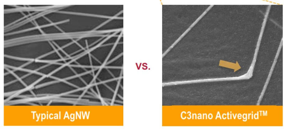
Silver nanowires are expected to become the new gold standard in touchscreen displays, delivering a bounty of benefits at reduced cost. The wires are usually developed and suspended in a fluid. The resultant ink is used to coat roll-to-roll plastic film substrates to create transparent conductive films of varying sheet resistances. Silver nanowires can also be coated on glass or other substrates but roll-to-roll film is most popular. The nanowires are a few tens of nanometers in diameter and a few tens of micrometers in length. When coated on a plastic substrate (usually PET), these high-aspect-ratio (1,000:1) silver nanowires, overlap to create a highly conductive, yet transparent network. See Figure 1. This relatively sparse network of high aspect ratio silver nanowires allows light to pass through with high transmission rates. State of the art conductive films using silver nanowires now have less than 0.2% delta haze, which is as good or better than ITO.

Meeting Touchscreen Requirements

Sheet resistance requirements for transparent conductors vary by application and touchscreen size. The conductivity requirements for a 30-inch monitor are significantly higher than that of a touchscreen used in a four-inch mobile phone. Touchscreen applications require highly transmissive materials for clear visibility; excellent conductivity to ensure fast touch response: and thin, light materials for sleek, aesthetically pleasing end products, all at a low cost. These requirements are constantly evolving.

Today, device makers are looking for conductivity below 70W/sq to make their touchscreens more responsive and further improve the user experience. For large area touchscreens in devices, such as 30-inch monitors or 42” electronic writing boards, higher conductivity is essential for a fast response time with the ability to detect 10-finger touch. For mobile devices like laptops and smartphones, film-based transparent conductors are in demand to create thinner, lighter and stronger touchscreens. With flexible displays on the horizon, transparent conductors will need the ability to be bent or rolled. Most importantly, transparent conductor prices must be low enough to encourage mass production of touch-enabled consumer electronic devices.

Transmission vs. Conductivity

High transmission (greater than 90 percent) along with low resistance (20 to 70W/sq) allows for 10-finger touch—the key to a great user experience. This is particularly true for laptops, All-In-One (AIO) computers, and other large-area capacitive touchscreens. Higher transmission also improves battery life per charge in mobile devices and creates brighter displays since the touch sensor does not impede light as much.

For sheet resistances of less than 130W/sq, traditional transparent conductors like ITO are only available on glass as their annealing temperature is too high and will damage plastic substrates. Higher conductivity with traditional methods is obtained by depositing a thicker layer of transparent conductor on a glass substrate, which takes more time to deposit, thus reducing throughput.

In contrast, silver nanowire ink can be coated at around 100° C—much lower than the softening temperatures of plastic films. Mass production throughput is also consistently high, regardless of sheet resistance requirements. For lower sheet resistance, product designers need only apply a thicker coating of silver nanowire ink at the same coating speed (hence same throughput).

Pattern Visibility and Moiré

Moiré effect occurs when the eye sees a set of lines or dots over another set of lines or dots. This visual image can considerably degrade the quality and resolution of images, particularly on a touchscreen. Silver nanowires have no moiré issues and almost no pattern visibility due to the random distribution of the nanowires.

Weight And Thickness

Nobody wants today’s consumer electronic devices to look like yesterday’s clunky machines. Tablet and laptop devices are becoming increasingly thinner and stationary devices like monitors and kiosks are becoming sleek and aesthetically pleasing, driving demand for thinner, lighter components. Electronic components with reduced mass tend to be more rugged and durable.

ITO is usually deposited on glass, resulting in a fragile, heavy glass touch sensor that is about 0.7 – 1.5 mm thick. In comparison, a silver nanowire film-based touch sensor is only 0.2 – 0.4mm thick. Silver nanowire sensors on film are roughly 45 percent lighter and 50 percent thinner than its ITO counterpart, giving film-based silver nanowire sensors a big advantage.

Flexible, Wearable Displays And Touchscreens

Necessity being the mother of invention, it didn’t take long for display manufacturers to realize that too many mobile phone users were sitting on and cracking their touchscreens. Result: touchscreens are becoming increasingly flexible. In fact, touchscreens have become so flexible that you may soon be able to fold or roll up your smartphone or tablet when not in use.

Flexibility is clearly the next big trend in touchscreens and displays, allowing for enhanced portability, durability, and unique designs. Imagine unbreakable phone screens that would flex instead of shattering when dropped, the ability to fold your seven-inch tablet so that it fits in your pocket, or displays that wrap around your arm, a pillar or building. Products like these are slowly becoming a reality and are driving demand for flexible, bendable and rollable touchscreens.

Touchscreens Ideal for Large Area Displays

Often seen in corporate meeting rooms, executive or customer briefing areas, huddle spaces, and college/universities, large touch screen based devices have become increasingly popular. They are popular as Ideation platforms, they make for great electronic writing, sharing, real-time collaboration and offer better security than the traditional white board where someone takes a picture before it is erased. In these types of devices, there is a need for highly transparent and highly conductive touch sensors and silver nanowires play an enabling role in such applications.

Touchscreens Help Drive Automotive Market

Automotive manufacturers are integrating touchscreens into center stack displays, navigation systems, human-machine interfaces (HMIs), keyless entry, and rear-seat entertainment systems. According to a recent study, shipments of touchscreen displays for automotive applications rose sharply in 2018. This trend is expected to increase over the next four years, with projected shipments exceeding 65 million units in 2021.

Conclusion

For emerging touchscreen applications, including large area touchscreens, as well as flexible display applications, silver nanowires offer a significant advantage, both in cost and performance. Currently used in several consumer products, silver nanowire material offers lower manufacturing and per-unit costs and makes scaling much easier. Roll-to-roll processed silver nanowire transparent conductors are the clear choice for new production facilities that need high throughput and easy processing, as well as for device manufacturers that need a thin, light, flexible material to deliver high performance for innovative devices.

Related Content

Press Release
C3Nano Announces Scaling-Up of its Ultra-Nanowires™ Product Line: Plating Technologies Propel Nanowires to a New Level and Enable Novel Industrial Applications
More Robust and Reliable Nanowire Opens Countless New Conductive Composite and Coating Applications for Smart Adhesives, Aerospace, Anti-Static, Shielding, Biocompatibility, Heating, Automotives and Cleantech...
Press Release
C3Nano Announces Activegrid™ Room Temperature Curing Conductive Ink, Transforming the Advances Materials and Smart Surface Industry
New Low Temperature Process with Electrically Conductive Inks Unlocks Unprecedented New Application Possibilities for Life-Sciences, Packaging, Consumer Electronics, Automotive and Disposable Commodities October 04,...
Press Release
ACS announces winner of the ACS Central Science Disruptors & Innovators Prize
WASHINGTON, July 2, 2020 — The American Chemical Society (ACS) Publications Division and ACS Central Science are pleased to announce the winner of theACS Central Science Disruptors...
Press Release
C3Nano专利 情况说明
作为下一代透明导电油墨和薄膜的性能领导者,C3Nano公司就近期在中国的专利相关纠纷进展情况发表正式声明。
Press Release
C3Nano IP Positioning Statement
C3Nano Inc., the performance leader in next-generation, transparent conductive inks and films, would like to set the record straight with regard to recent IP developments...
Press Release
C3Nano FAQ With Regard to Its IP
FAQ Analysis: June 2020 1. Explain the difference between invalidation versus infringement. 2. Is C3Nano’s fusing technology/IP still protected? 3. The Cambrios press release...

C3Nano’s Dr. Ajay Virkar to Present at SID’s Display Week 2018

HAYWARD, Calif.–(BUSINESS WIRE)–C3Nano, Inc., the performance leader in transparent conductive inks and films for the touch sensor, display and flexible electronics industry, announced today that co-founder and CTO, Dr. Ajay Virkar will present at SID’s Display Week 2018 symposium and conference, taking place at the Los Angeles Convention Center, Los Angeles, CA., May 20-25, 2018.

The presentation, ‘ActiveGrid™: A Flexible Solution Processed Transparent Conductor with Excellent Optical Properties’ will highlight C3Nano’s unique technology, utilizing novel chemistries and materials to create the highest performing, flexible transparent conductor. The underlying physical chemistry, thermodynamics and kinetics of ActiveGrid™ formation will also be described, as will advanced technologies related to manipulating and improving optics and flexibility. May 23, 2018, 10:40am, LA Convention Center, Room 515B.

C3Nano‘s high-performing flexible conductor utilizes NanoGlue™ a proprietary chemical sintering agent that fuses metallic nanowires into a nanoscale metallic grid. With less material, ActiveGrid™ achieves low resistances and enables ultra-low haze transparent conductors for a variety of touch sensors and displays. Haze values of 0.2 percent at 50 ohm/sq and 0.1% at 70 ohm/sq have been achieved for the transparent conducting layer.

ActiveGrid™ Inks and Films are valued for their performance, durability, flexibility, and processability; they are utilized for a variety of applications ranging from touch sensors OLED lighting, EMI shielding, and solar cells to biotechnology uses.

Dr. Virkar completed his Ph.D. in chemical engineering from Stanford University and his undergraduate degree from the University of Illinois. Virkar was awarded the Springer Prize for his thesis research and the Melvin P. Klein Prize for his studies of structure-property relationships of ultra-thin films in collaboration with the Stanford Linear Accelerator. He has co-authored thirteen technical papers and has 20 patents, issued or pending.

About C3Nano, Inc.

C3Nano made headlines in 2017 when it closed $18 million in equity financing, bringing C3Nano’s total equity financing to over $40 million. Founded in 2010 as a spinout from Professor Zhenan Bao’s chemical engineering laboratory at Stanford University, C3Nano is an advanced materials company focused on developing new materials and chemistries for a wide range of electronic applications.

About Display Week 2018

The 55th annual SID International Symposium, or Display Week 2018, is the premier gathering of system integrators, designers, consumers, scientists, engineers and manufacturers in the field of electronic information displays.

Related Content

Press Release
C3Nano Announces Scaling-Up of its Ultra-Nanowires™ Product Line: Plating Technologies Propel Nanowires to a New Level and Enable Novel Industrial Applications
More Robust and Reliable Nanowire Opens Countless New Conductive Composite and Coating Applications for Smart Adhesives, Aerospace, Anti-Static, Shielding, Biocompatibility, Heating, Automotives and Cleantech...
Press Release
C3Nano Announces Activegrid™ Room Temperature Curing Conductive Ink, Transforming the Advances Materials and Smart Surface Industry
New Low Temperature Process with Electrically Conductive Inks Unlocks Unprecedented New Application Possibilities for Life-Sciences, Packaging, Consumer Electronics, Automotive and Disposable Commodities October 04,...
Press Release
ACS announces winner of the ACS Central Science Disruptors & Innovators Prize
WASHINGTON, July 2, 2020 — The American Chemical Society (ACS) Publications Division and ACS Central Science are pleased to announce the winner of theACS Central Science Disruptors...
Press Release
C3Nano专利 情况说明
作为下一代透明导电油墨和薄膜的性能领导者,C3Nano公司就近期在中国的专利相关纠纷进展情况发表正式声明。
Press Release
C3Nano IP Positioning Statement
C3Nano Inc., the performance leader in next-generation, transparent conductive inks and films, would like to set the record straight with regard to recent IP developments...
Press Release
C3Nano FAQ With Regard to Its IP
FAQ Analysis: June 2020 1. Explain the difference between invalidation versus infringement. 2. Is C3Nano’s fusing technology/IP still protected? 3. The Cambrios press release...

Does C3Nano Have the Technology that Will Kill ITO?

original post from Ken Werner for Display Daily, 10/12/17

The last time we took a serious look at technologies for replacing ITO in transparent conductors, Cambrios was the leading purveyor of silver nanowires (AgNWs). Cambrios was battling metal mesh technology to see who would lead in displacing ITO. But ITO refused to be displaced, and Cambrios found it had invested heavily to prepare itself for a market that was developing too slowly.

Cambrios, painfully, had to liquidate itself in a pennies on the dollar auction. And it was then that the calvary — the Taiwanese calvary — rode to the rescue. Leading touch-panel manufacturer TPK, which had been a customer of Cambrios, bought up the important pieces. Now, TPK is building fabs for manufacturing AgNW ink with the Cambrios technology and is investing heavily.

But with Cambrios now part of TPK, is there an opening for an independent AgNW producer, especially if has a technology it claims is superior to that of Cambrios?

Before it was ingested by TPK, Cambrios was not the only maker of silver-based inks for flexible, transparent conductors, even though it was the largest one. Others ran into the same problem as Cambrios (they were ready but the market wasn’t), and some interesting technologies went by the board. (TPK Will Produce Silver Nanowire Products – subscription required)

A small development-stage company — C3Nano — continued to develop its technology and is now sampling its ink and preparing for pilot roll-to-roll film manufacturing.

(See C3Nano Buys Silver Nanowire MakerC3Nano and Nissha Partner on Silver Nanowire Conductive Film and Silver Nanowires Get Large – subscription needed for our previous coverage). The company’s novel IP is for ActiveGrid ink, which incorporates materials that are attracted to the places where the AgNWs cross as the ink is tried. They effectively weld the AgNWs where they cross, producing much better conductivity, even with a lesser concentration of AgNWs. This produces less haze in bright ambient conditions than is true of conventional AgNW solutions. The process depends on a sophisticated system that depends on reduced surface free energy at the crossing points. To simplify things for non-chemists, the company calls it NanoGlue Technology.

C3Nano reduces the resistance between nanowires.

Other than haze, transparent conductors are characterized by their bendability and their trade-off between optical transmissivity and conductivity. You would certainly like to have a conductive film that simultaneously has very low sheet resistance and and very high transmissivity, but the two trade off against each other. C3Nano’s NanoGlue permits a lower density of AgNWs which permits a high transmissivity as well as low haze. C3Nano says ActiveGrid has a sheet resistance of between 30 and 100 ohms/square, as compared to 50 to 100 for conventional AgNW technologies. ActiveGrid transmittance is 90-92%, compared to 89-91% for conventional, and haze is 0.2-1.0% compared to 0.8-1.5% for conventional. These optical properties include the substrate.

Although the news of ITO’s death has been exagerated, projections for the market penetration of ITO replacements finally look encouraging. Penetration was less than 20% in 2017, but should reach 50% in 2021 and rise thereafter, according to a 2016 Touch Display Research report.

So, does all of this look good to investors? In a word, yes. C3Nano had a goal of $10 million for its Series D equity financing round this summer, and wound up with $21 million. Among the investors is Nissha Printing, which C3Nano calls a “key development partner for advanced touch sensor films.” Hitachi Chemical is another partner.

This is interesting. We’ll keep an eye on C3Nano and let you know what we see.

***

Ken Werner is Principal of Nutmeg Consultants, specializing in the display industry, manufacturing, technology, and applications, including mobile devices and television. He consults for attorneys, investment analysts, and companies re-positioning themselves within the display industry or using displays in their products. He is the 2017 recipient of the Society for Information Display’s Lewis and Beatrice Winner Award. You can reach him at kwerner@nutmegconsultants.com.

Related Content

Press Release
C3Nano Announces Scaling-Up of its Ultra-Nanowires™ Product Line: Plating Technologies Propel Nanowires to a New Level and Enable Novel Industrial Applications
More Robust and Reliable Nanowire Opens Countless New Conductive Composite and Coating Applications for Smart Adhesives, Aerospace, Anti-Static, Shielding, Biocompatibility, Heating, Automotives and Cleantech...
Press Release
C3Nano Announces Activegrid™ Room Temperature Curing Conductive Ink, Transforming the Advances Materials and Smart Surface Industry
New Low Temperature Process with Electrically Conductive Inks Unlocks Unprecedented New Application Possibilities for Life-Sciences, Packaging, Consumer Electronics, Automotive and Disposable Commodities October 04,...
Press Release
ACS announces winner of the ACS Central Science Disruptors & Innovators Prize
WASHINGTON, July 2, 2020 — The American Chemical Society (ACS) Publications Division and ACS Central Science are pleased to announce the winner of theACS Central Science Disruptors...
Press Release
C3Nano专利 情况说明
作为下一代透明导电油墨和薄膜的性能领导者,C3Nano公司就近期在中国的专利相关纠纷进展情况发表正式声明。
Press Release
C3Nano IP Positioning Statement
C3Nano Inc., the performance leader in next-generation, transparent conductive inks and films, would like to set the record straight with regard to recent IP developments...
Press Release
C3Nano FAQ With Regard to Its IP
FAQ Analysis: June 2020 1. Explain the difference between invalidation versus infringement. 2. Is C3Nano’s fusing technology/IP still protected? 3. The Cambrios press release...

C3Nano’s Dr. Virkar Presents at ICMAT 2017

HAYWARD, Calif.–(BUSINESS WIRE)–C3Nano, Inc., the performance leader in transparent conductive inks and films for the touch sensor, display and flexible electronics industry, announced today that co-founder and CTO Ajay Virkar will present at the International Conference on Materials for Advanced Technologies taking place at Suntec, Singapore, June 18-23, 2017.

Virkar, an invited presenter, will discuss C3Nano’s unique technology, utilizing novel chemistries and materials to create the highest performing, flexible transparent conductor, ActiveGrid™. The underlying physical chemistry, thermodynamics and kinetics of ActiveGrid™ formation will also be described. Advanced technologies related to manipulating and improving optics and flexibility will also be covered.

ActiveGrid™ Inks and Films, are valued for their performance, durability, flexibility, and processability; they are utilized for a variety of applications ranging from touch sensors OLED lighting, EMI shielding, and solar cells to biotechnology uses.

Dr. Virkar completed his PhD in chemical engineering from Stanford University and his undergraduate degree from the University of Illinois. Virkar was awarded the Springer Prize for his thesis research and the Melvin P. Klein Prize for his studies of structure-property relationships of ultrathin films in collaboration with the Stanford Linear Accelerator. He has co-authored thirteen technical papers and has 20 patents, issued or pending.

About C3Nano, Inc.

C3Nano made headlines earlier this year as it closed $18 million in equity financing. The latest financing was led by existing investor GSR Ventures, new investors Nissha Printing Co., Ltd. and Xinjiang Guoli Minsheng Equity Investment Co., Ltd. Other investors included Phoenix Venture Partners, and several undisclosed investors, including a leading Silicon Valley technology company. Building on the Series C financing led by Hitachi Chemical and Nagase America, the new round brings C3Nano’s total equity financing to over $40 million since its inception.

Founded in 2010 as a spinout from Professor Zhenan Bao’s chemical engineering laboratory at Stanford University, C3Nano is an advanced materials company focused on developing new materials and chemistries for a wide range of electronic applications.

About ICMAT 2017

The International Conference on Materials for Advanced Technologies, now in its ninth year, is an important biennial organized by the Materials Research Society of Singapore (MRS-S) and takes place at Suntec Singapore.

Related Content

Press Release
C3Nano Announces Scaling-Up of its Ultra-Nanowires™ Product Line: Plating Technologies Propel Nanowires to a New Level and Enable Novel Industrial Applications
More Robust and Reliable Nanowire Opens Countless New Conductive Composite and Coating Applications for Smart Adhesives, Aerospace, Anti-Static, Shielding, Biocompatibility, Heating, Automotives and Cleantech...
Press Release
C3Nano Announces Activegrid™ Room Temperature Curing Conductive Ink, Transforming the Advances Materials and Smart Surface Industry
New Low Temperature Process with Electrically Conductive Inks Unlocks Unprecedented New Application Possibilities for Life-Sciences, Packaging, Consumer Electronics, Automotive and Disposable Commodities October 04,...
Press Release
ACS announces winner of the ACS Central Science Disruptors & Innovators Prize
WASHINGTON, July 2, 2020 — The American Chemical Society (ACS) Publications Division and ACS Central Science are pleased to announce the winner of theACS Central Science Disruptors...
Press Release
C3Nano专利 情况说明
作为下一代透明导电油墨和薄膜的性能领导者,C3Nano公司就近期在中国的专利相关纠纷进展情况发表正式声明。
Press Release
C3Nano IP Positioning Statement
C3Nano Inc., the performance leader in next-generation, transparent conductive inks and films, would like to set the record straight with regard to recent IP developments...
Press Release
C3Nano FAQ With Regard to Its IP
FAQ Analysis: June 2020 1. Explain the difference between invalidation versus infringement. 2. Is C3Nano’s fusing technology/IP still protected? 3. The Cambrios press release...